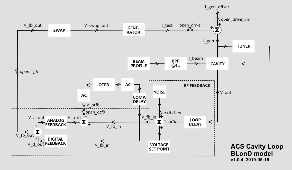
LHC Cavity Loop
- Authors
Helga Timko

The interaction of the LHC cavity loop with the beam is modelled on a turn-by-turn basis. All arrays inside the class
blond.llrf.cavity_feedback.LHCCavityLoop are complex arrays with a memory of exactly 2 turns (previous and
present). The signals are digitised with a sampling time \(T_s\) that adapts to the revolution period to have
exactly
N = int(self.rf.harmonic[0, 0]/10)
samples over one turn. The feedback is pre-tracked without beam.
STEP 1: Calculate RF beam current
The RF beam current is calculated for the entire turn, based on the beam profile \(\lambda_k\), where the sampling time is typically much smaller than T_s.
STEP 2: Cavity-generator-beam interaction
Within one turn, the update of parameters happens sample by sample, for \(n = 0...N-1\). First, the antenna voltage measured in the RF cavity \(V_{\mathsf{ant}}\) is updated based on the time evolution derived in [JT2011]
Here \(I_{\mathsf{gen}}\) is the generator forward current, \(I_{\mathsf{beam,RF}}\) is the RF beam current, \(R/Q\) is the cavity’s ratio of shunt impedance and quality factor, \(Q_L\) the loaded quality factor, \(\omega\) the rf frequency, and \(\Delta \omega \equiv \omega_c - \omega\) the detuning of the cavity w.r.t.the central frequency \(\omega_c\). In the discrete implementation, the equation reads as follows:
where the upper indices denote the sample number.
STEP 3: RF feedback response
The RF feedback acts on the difference between measured antenna voltage and required set point voltage \(V_{\mathsf{set}}\):
where the overall loop delay \(\tau_{\mathsf{loop}}=650 \mathsf{ns}\) is taken into account in the antenna signal delayed by \(n_{\mathsf{loop}} \equiv int(\tau_{\mathsf{loop}})/T_s\).
Analog feedback
The analog feedback has a gain \(G_a\) at high frequencies and in Laplace domain its transfer function is:
where \(X(s)\) and \(Y(s)\) are the input and output signals, respectively. In the LHC, the typical delay is \(\tau_a = 170 \mathsf{\mu s}\) (based on AC coupling at demodulator exit), and the optimum gain for a flat closed- loop response is
which for a loop delay of \(\tau_{\mathsf{loop}} = 650 \mathsf{ns}\) results in \(G_a = 6.79 \times 10^{-6} \mathsf{\frac{A}{V}}\). Note that \(G_a\) converts the voltage signal to a current signal.
In discrete time domain, the output signal \(y(t)\) is calculated from the input signal \(x(t)\) as follows:
Digital feedback
The digital feedback, opposite to the analog feedback, has a high gain at low frequencies,
where the digital gain is typically \(G_d=10\), and the dephasing between the analog and digital feedbacks is to be minimized, \(\Delta \varphi_{\mathsf{ad}} \approx 0\).
In discrete time domain, the signal reads as
One-turn feedback
There is the possibility to switch on the one-turn feedback to boost the gain of the analog feedback. On the branch of the one-turn feedback (OTFB), there is a delay that is complementary to the total loop delay as seen by the OTFB \(\tau_{\mathsf{otfb}}\), \(T_0 - \tau_{\mathsf{otfb}}\), where \(T_0\) is the revolution period in that turn.
The response of the one-turn feedback itself reads as follows:
where \(G_o = 10\) and \(\alpha=15/16\) usually.
In time domain, the signal from the previous turn is used to construct the signal at the current turn,
Both at the input and the output, an AC coupling ensures that unwanted frequencies are filtered out,
where the time constant is around \(\tau_o=110 \mathsf{\mu s}\).
In time domain, this reads as
In addition, a 63-tap finite-impulse response (FIR) filter is used to limit the bandwidth of the overall response.
The numerical implementation thus consists of the following four steps, in the below-mentioned order:
AC coupling at input on the signal of the previous turn, combined with OTFB delay \(T_0 - \tau_{\mathsf{otfb}}\) at input,
where \(N = \mathsf{int}(T_0/T_s)\) and \(n_{\mathsf{otfb}} = \mathsf{int}(\tau_{\mathsf{otfb}}/T_s + n_\mathsf{taps} - 1)/2)\), with \(n_\mathsf{taps}\) being the number of taps of the FIR filter,
OTFB response,
FIR filter response; N.B. this introduces an extra delay of \((n_\mathsf{taps} - 1)/2\) which is already compensated in step 1.
AC coupling at output.